Class 12

31. Semiconductor & Electronic Devices question bank (Physics)

Practice 256 free Class 12 Physics - 31. Semiconductor & Electronic Devices questions with answers and step-by-step solutions.

Q1.

The depletion layer in the \(p\)-\(n\) junction region is caused by  

(A)
drift of holes
(B)
diffusion of charge carriers
(C)
migration of impurity ions
(D)
drift of electrons
Show answer & solution
Verified Answer & Solution Locked
Sign in to your free student account to reveal verified answers, instant hints, and detailed explanations.
Sign in to view
Q2.

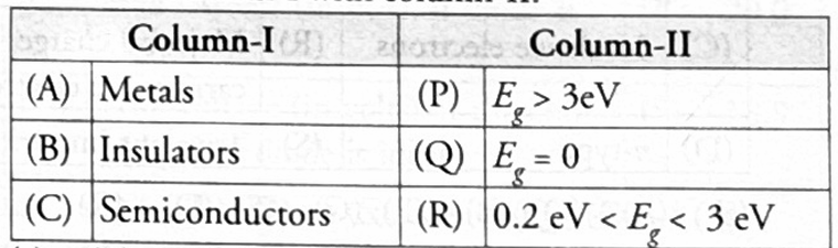
Match the column-I with column-II  

(A)
(A) – (P); (B) – (Q); (C) – (R)
(B)
(A) – (R); (B) – (P); (C) – (Q)
(C)
(A) – (Q); (B) – (P); (C) – (R)
(D)
(A) – (R); (B) – (Q); (C) – (P)
Show answer & solution
Verified Answer & Solution Locked
Sign in to your free student account to reveal verified answers, instant hints, and detailed explanations.
Sign in to view
Protected Questions

Unlock All 256 Questions in 31. Semiconductor & Electronic Devices

Log in or sign up free to access every question with complete solutions, create chapter practice tests, and track your performance.

Sign up free to access all 256 questions

Unlock every 31. Semiconductor & Electronic Devices question, generate papers, and practice at your own pace.